Voice08
Contents
- 1 HC08 Project Development with MC68HC908JL16 using 'C' and assembly
- 2 Voice08 project expences
- 3 Debugging with Eclipse based Codewarrior
- 4 References
- 5 S19 FILE
- 6 Source code
- 7 Source code Disassembly
- 8 MC68HC908JL16
- 9 MC9S08GT16
- 10 CodeWarrior
- 11 Serial Memory
- 12 Links
- 13 Text to speech
- 14 2011.07.27 TODO DONE
- 15 2011.07.28
- 16 2011.08.23
- 17 2011.08.29
- 18 2011.08.30
- 19 2011.08.31
- 20 2011.09.01
- 21 2011.09.02
- 22 2011.09.03
- 23 2011.09.04
- 24 2011.09.05
- 25 2011.09.06
- 26 2011.09.07
- 27 2011.09.20
- 28 2011.09.21
- 29 2011.10.05 Intelco meeting
- 30 2011.10.27
- 31 HCS08 (BDM) Debug and Flash-programming Tools
HC08 Project Development with MC68HC908JL16 using 'C' and assembly
This is a small-voice-announcement board, extending INTP0900 (MC68HC908JL16) hands-free elevator telephone board.
The firmware will be included in the existing firmware of the INTP0900.
Alternatively a local CPU will handle the voice-memories
- INTP0900

Voice08 project expences
| item |
description |
Manufacturer |
part-number |
CASE |
Digikey code |
Mouser code |
quantity |
DIGIKEY PRICEprice(USD) |
price(EU) |
BAKIS PRICE(EU) |
total (EU) |
TO ORDER | ORDERED | EXPECTED | DELIVERED |
| 1 |
SPI SRAM 32K x 8 |
Microchip |
23K256 |
|
23K256-I/P-ND |
|
4 |
1.66 |
1.17337 |
1.66 |
4.7 |
X | 2011.07.25 | 2011.08.22 | 2011.08.24 |
| 2 |
SPI EEPROM 64K x 8 |
Microchip |
25LC512-I/P |
|
25LC512-I/P-ND |
|
4 |
2.64 |
1.86906 |
2.64 |
7.48 |
X | 2011.07.25 | 2011.08.22 | 2011.08.24 |
| 3 |
USBMULTILINKBDME |
Freescale |
USBMULTILINKBDME |
|
USBMULTILINKBDME-ND |
|
0 |
99 |
70.0898 |
|
|
|
|
|
|
| 4 |
USBMULTILINK08E |
Freescale |
USBMULTILINK08E |
|
USBMULTILINK08E-ND |
|
0 |
99 |
70.0898 |
|
|
|
|
|
|
| 5 |
FRAM 32K x 8 |
Everspin |
MR25H256 |
|
819-1015-ND |
|
1 |
5.66 |
5.66 |
5.66 |
5.66 |
X | 2011.07.25 | 2011.08.22 | 2011.08.24 |
| 6 |
FRAM 128K x 8 |
Everspin |
MR25H10 |
|
819-1014-ND |
|
1 |
9 |
9 |
9 |
9 |
X | 2011.07.25 | 2011.08.22 | 2011.08.24 |
| |
|
|
|
|
|
|
|
|
|
|
|
|
|
|
|
| |
2ND ORDER |
|
|
|
|
|
|
|
|
|
|
|
|
|
|
| |
|
|
|
|
|
|
|
|
|
|
|
|
|
|
|
| 7 |
SPI SRAM 32K x 8 |
Microchip |
23K256 |
8-DIP |
23K256-I/P-ND |
|
6 |
1.66 |
|
1.66 |
|
X |
2011.09.08 |
2011.09.13 |
|
| 8 |
SPI EEPROM 64K x 8 |
Microchip |
25LC512-I/P |
8-DIP |
25LC512-I/P-ND |
|
3 |
2.64 |
|
2.64 |
|
X |
2011.09.08 |
2011.09.13 |
|
| 9 |
IC MCU 16K FLASH 8MHZ 28-DIP |
Freescale |
MC908JL16CPE |
28-DIP |
MC908JL16CPE-ND |
|
2 |
3.35 |
|
3.35 |
|
X |
2011.09.08 |
2011.09.13 |
|
| 10 |
IC MCU 16K FLASH 2K RAM 44-QFP |
Freescale |
MC9S08GT16ACFBER |
44-QFP |
MC9S08GT16ACFBERCT-ND |
|
4 |
3.84 |
|
3.84 |
|
X |
2011.09.08 |
2011.09.13 |
|
| 11 |
IC MCU 8BIT 8K FLASH 20-DIP |
Freescale |
MC9S08SH8MPJ |
20-DIP |
MC9S08SH8MPJ-ND |
|
2 |
2.3 |
|
2.3 |
|
X |
2011.09.08 |
2011.09.13 |
|
Debugging with Eclipse based Codewarrior

References
- 300-page MC9S08GT16A datasheet at Freescale Product page
- page 125 ICG Internal Clock Generator (S08ICGV4)
- page 131 ICGC1 register
- page 133 ICGC2 register
- page 154 TPM
- page 158 TPMxSC
- page 160 TPMxMOD
- page 161 TPMxCnSC
- page 162 TPM1C1V
- MC9S08GT16A ADC is named ATD (similar to HC12 series)
- page 222 ATD
- page 225 ATD registers
- page 228 ATDSC
- page 229 ATDPE
- page 266 Run current
- Pereira
- page 197 ICGC2 register
- page 255 PWM example
- page 217 Low power techniques
- SPI-Bit-Banging from chapter11-example3 ScTec Downloads
- page 254 PWM Led Dimmer for ICG and TPM configuration
S19 FILE
Last update 2011.09.02.20:08
S01200006578616D706C6531315F332E616273A9
S123C0008B899EFE05F6AF019EFF05888A81A7FCC6C0854C95E701C6C0844CF732C0862030
S123C0201F898BF687E6024C9EE706E603EE018A4C20037FAF014BFB9E6B05F78A88AF047D
S123C0409E6B02DD9E6B01D932C088898BADB1974C9EE703ADAA4C9EE7044A2603510018B2
S123C060AD9E878AAD9A972005AD95F7AF019E6B04F79E6B03F320D5A7068145020F94ADB7
S123C0808DCCC3250001C08AC4400100008F000000006E080F6E400B6E84036E02546EE037
S123C0A0506E01516E0860AE648C35636E28685F356916301C305A35333F385F35396E015E
S123C0C0336EB8349A8187A7FEB62B8C979EFF019EE603B72D9EFF01A70381A7FEB62B8CA0
S123C0E0979EFF01A6FFB72DB62DC701099EFF01A702818987957D2602170C4B021F00A683
S123C10001ADC395E601ADBE957D2602160CF64B021E00A70281898795E604C7010AE60590
S123C120C7010B7D2602170CF64B021F00A602AD95C6010AAD90C6010BAD8B95E601AD864D
S123C140957D2602160CF64B021E00A70281878B86C7010ACF010B957D2602170CF64B020F
S123C1601F00A603CDC0C6C6010ACDC0C6C6010BCDC0C6CDC0DB957D2602160CF64B021E32
S123C18000C60109C701088A811D08A606CDC0C61C0881898BA7FEADF095E602C7010AE69C
S123C1A003C7010B1D08A602CDC0C6C6010ACDC0C6C6010BCDC0C6956F017F95EE018CD6D2
S123C1C0010DCDC0C6956C0126017C9EFE0165008025E81C08A70481A7FA1D30956F017F04
S123C1E0A607879EFE029F8B88CDC4348A898A979EFF05956F036F02956C0326026C029E6C
S123C200FE036507D025F19EFE05657FFF220C898BAE808CA601CDC26CA7029EFE05657F77
S123C220FF230F898B86A08087AE808C4FCDC26CA7029EFE05CDC193956C0126017C9EFED8
S123C24001650200259A1C30A706818B86C7010ACF010B1D08A603CDC0C6C6010ACDC0C636
S123C260C6010BCDC0C6CDC0DB1C0881898B87A7FE9EE608C7010A9EE609C7010B650080A5
S123C2802306AE808C9EFF04AE414FCDC0F3AE41A601CDC0F3956D022602170CE6024B02BE
S123C2A01F00A603CDC0C6C6010ACDC0C6C6010BCDC0C6956F017F2013CDC0DB95EE018CE7
S123C2C0C60109D7010D956C0126017C9EFE049EF30122E5956D022602160CE6024B021E26
S123C2E000AE014FCDC0F3AE019FCDC0F3A705818B1F30A601C70107C6018D270445018D1F
S123C3007A150014008A806E50283F2A81A622C718024FC7180A6E0149818BB62BB62D4FE4
S123C320C7018E8A80ADE6CDC092ADDB14001C08160C1E0009000D45FFFF960100898A964E
S123C34001021E5008000F5F8C960100960102A601C701061F5045FFFF960104504FCDC048
S123C360F3C601074A2703CCC4314FC701073201002748BE51A37F23404501006D01260194
S123C3807A6A01BE52CF010C8C3569320100657FFF230F898B86A08087CE010C4FCDC11647
S123C3A0A702320100657FFF220C898BCE010CA601CDC116A7026E01512041320102273CF0
S123C3C04501026D0126017A6A01320102657FFF230A8B86A080878A4FCDC14E320102654B
S123C3E07FFF2205A601CDC14ECE01088C35693201022608A601C70106CDC1D83201046536
S123C400000026024F65A601C4010627244501046D0126017A6A01320104CDC24BCE0109D2
S123C4208C3569320104650001240645FFFF960104CCC3619E6D03270648599E6B03FA81D6
S10FC440000601007FFF7FFFFFFF0000EB
S105FFE0C31A3E
S105FFEEC2F05B
S105FFFEC07BC2
S9030000FC
Source code
LAST UPDATE 2011.09.02.19:31
//V007
//stop tick during EEPROM write
//Rename BUSY_LED to TP1, Do not use anywhere except...
//Use TP1 only in TICK interrupt
//increase TICK to 4.4KHz, WE can stay with this.
//SAMPLING_RATE 0x01 0xB8
//4.9 KHz Fails to write in SRAM  ??? WHY ???
//CONSUMPTION IS 3.5 mA(EEPROM WRITE AND READ) AND 4 mA (SRAM WRITE AND READ) *** AT 2 V ***
//We have to go with 2V VDD. It is inside the low VDD limits of all ICs
//Still with zero input recording is very quiet :)
//With audio connection to PC audio output and no sound we have "background" noise ?????? WHY ???????
//The used sound from PC has too many high frequency components to 's'. It is digitally synthesized.
//In PCB To use 2 stages better passive filter in output (now single stage) and to input (now without filter)
//Tested input single stage low-pass filter (Anti-aliasing) 200nF+3.9K, Output filter (single stage low-pass for PWM) 200nF+1K  <<<<Quality is improved, no 'background' noise, 's' sounds better
//Some metallic tone in voice still exists
//Input DC bias voltage set to 500 mV
//


//V006
//ICGC2 = MFDx4 | RFD_DIV2;          instead ICGC2 = MFDx10;   in V005
//spi_wr(), spi_read() all delays removed
//SPIBR = SPI_PRE1 | SPI_DIV2;
//SAMPLING_RATE 0X02 0X00 **3.9 KHz**, difficult to increase
//Test RECORDING with no input signal is very silent :)

//V005 ONLY MINOR CHANGES (REMOVE UNUSED VARIABLES)


//V004 FROM V002B
//SPI working SPTEF can not be read. for read it does not matter,  --->Is transmit register empty, means register can accept data BUT TRANSMITION still ACTIVE!
//so no use as end of transmission
//affects only the last byte of every sector???
//For write matters when EEPROM sector is massively written. In this case the bytes go one after the other and not in the sampling-rate frequency
//*** During EEPROM writing, Can seen in oscilloscope that SPI clock still plays after EEPROM CS is de-activated (=high)***
//Some delay (~2us) needed then
//Can not use the tick as it is in the 200us period
//SPRF tested and did not work
//SPRF interrupt tested, did not work
//Remain with the delay <<< does not matter, with lower BUSCLK have to remove the delays....check higher versions


//V002 GPIO PORTS INITIALISATION NOW CORRECT


//NX	2011.08.30
//NX    Second SRAM 32KBytes (EEPROM is 64KBytes)
//NX    Doubles the message duration
//NX    Added to breadboard
//NX    Firmware updated
//NX    MODE switch added
//NX    Mode0 = Playback the EEPOM content
//NX    Mode1 = Record and Playback
//NX    STILL TODO:
//NX    ADD CD4094 functionality
//NX        Now using I/O lines for
//NX           CHIP SELECT of first SRAM
//NX            CHIP SELECT of second SRAM
//NX            CHIP SELECT of EEPROM
//NX    Create PCB
//NX            Schematic,PCB, Gerber,
//NX            CNC prototype
//NX            Solder and test

//NX 	2011.08.29
//NX    Recording with 4.9 KHz sampling rate video
//NX 	first time input ->ADC ->PWM so we can hear what is recorded
//NX    second time SRAM to audio, for debugging
//NX    third time EEPROM to audio. It is the stored recording
//NX    next times are repeats of EEPROM recording (debugging)

// NX 2011.08.27
// NX EEPROM functionality added

// NX 2011.08.26
// NX Successful test with 23K256

// NX 2011.08.22
// NX comments added

// NX 2011.07.16 Bit_banging SPI. YES IT WORKS
// Tested on MPR083 demo board with 9S08GT16A

#include <hidef.h> 	        /* for EnableInterrupts macro */
#include "derivative.h" 	/* include peripheral declarations */      // NX Codewarrior knows the used CPU from the project settings
#include "hcs08.h"

#define MODE 	PTAD_PTAD4					//NX PTE2 is mode input -->Record = 1, Playback = 0
#define MOSI      PTDD_PTDD0
#define MISO      PTCD_PTCD5
#define CLOCK     PTDD_PTDD1
#define SRAMSELECT0    PTDD_PTDD3			//NX PTD3 is Chip select for first sram chip (CHIP0)
#define SRAMSELECT1    PTAD_PTAD7			//NX PTE3 is Chip select for second sram chip (CHIP1)
#define EEPROMSELECT    PTCD_PTCD6 			//NX PTC6 is EEPROM CS
#define CD4094STROBE    PTDD_PTDD3          //<<<<<<<<<<<<<<<<<<<<<<<<<<<<<<<<<<<<<< DEFINE ALSO THIS BIT
#define TP1		PTAD_PTAD2
#define ANALOG_CH 0x01
#define KHZ_3_2     0x18
#define KHZ_4_3     0x12		//NX 0x12=4.3KHz
#define KHZ_4_9    0x10
#define KHZ_5_2    0x0F
#define KHZ_7_0     0x0B
#define KHZ_7_8   0x0A
#define SAMPLING_RATE_H 0x01
#define SAMPLING_RATE_L 0xB8
#define PWMFREQ_MFDx10_20KHZ 552
//#define PWM_FRQ 80
#define PWM_FRQ 100

//NX SPI SRAM and EEPROM 23K256, 25LC512
#define BYTE 0x01
#define PAGE 0x02
#define SEQUENTIAL 0x41		//NX 0100 0001 TO STATUS REGISTER

#define WRSR 0x01
#define WRITE 0x02
#define READ 0x03
#define WREN 0x06
#define WRDI 0x04
#define CE   0xC7
#define RDSR 0x05

#define SRAMCS     0x00
#define EEPROMCS  0x01
#define NOCS      0xFF

#define E_SELECT   EEPROMSELECT = 0;
//#define E_SELECT   spi_4094_wr(EEPROMCS);
#define E_UNSELECT EEPROMSELECT = 1;
//#define E_SELECT   spi_4094_wr(NOCS);
#define S_SELECT0   SRAMSELECT0   = 0;
//#define E_SELECT   spi_4094_wr(SRAMCS);
#define S_UNSELECT0 SRAMSELECT0   = 1;
//#define E_SELECT   spi_4094_wr(NOCS);
#define S_SELECT1   SRAMSELECT1   = 0;
//#define E_SELECT   spi_4094_wr(SRAMCS);
#define S_UNSELECT1 SRAMSELECT1   = 1;
//#define E_SELECT   spi_4094_wr(NOCS);

#define SRAM0 0					//NX To select more than one SRAM chips
#define SRAM1 1
#define EEPROM_PGSIZE 128		//NX Used to EEPROM page write
#define RECORD 1
#define PLAYBACK 0


//NX Global variables, Can be seen from debugger at any point
unsigned int wr_address =   0x7FFF;
unsigned int rd_address =   0x7FFF;
unsigned int eerd_address = 0xFFFF;
unsigned char SVAL;
unsigned char rdata;
unsigned char address_h, address_l;
unsigned char ADCVALUE;
unsigned char EEPROM_WRITTEN = 0;

unsigned char BUFFER[EEPROM_PGSIZE];

unsigned char GLOBAL_TOF = 0;

unsigned char delay;

unsigned char spi_busy;

void spi_sram_read_sector(unsigned int address,unsigned int size ,unsigned char sram_number);
void spi_eeprom_chiperase(void);

//*****************************************************************************************************************
// MCU initialization
void mcu_init(void)			// NX  initialize Ports, Clock, Timers, ATD (~ADC), ...Interrupts
{


  // NX PORTS AND ATD(=ADC)
  PTDDD = BIT_3;  							// NX CS0
  PTCDD = BIT_6;							// NX Output: PTC6   CS2
  PTADD = BIT_2 | BIT_7;					// NX Output: TP1 , CS1


  ATDPE = ANALOG_CH+0x01; // NX PortB.ANALOG_CH pin(s) --> analog input(s)
  ATDC  = 0xE0;		      // NX enable, justification-right, 8bit-resolution, left-is-unsigned, 0000-divide-2

  ATDSC = ANALOG_CH;	  // NX This write starts an new conversion, Using channel ANALOG_CH
                          // NX Read BIT7=CCF=ConversionCompleteFlag no-interrupt,single-conversion,channel-1

						  // NX TPM2 is used for PWM
  TPM2SC = 0X08;		  // NX TPM Clock Source to Prescaler Input IS Bus rate clock (BUSCLK) [page 158]
  TPM2MOD = PWM_FRQ;//0xFF;  // NX TPM2 counter maximum value Controls the PWM frequency. 0xFF-->78KHz, 1000-->20KHz. Reduce of consumption ~0.5mA, 552@MFDx10--->20KHz
  TPM2C1SC = TPM_PWM_HIGH;// NX Input Capture Output Compare
  TPM2C1V = 0x00;		  // NX Unlatch the Value register

						  // NX TPM1 is used for sampling rate timing
  //TPM1SC = 0X08;		  // NX TPM Clock Source to Prescaler Input IS Bus rate clock (BUSCLK) [page 158]
  TPM1SC |= BIT_3;		  // NX TPM clocked by BUSCLK
  TPM1SC |= BIT_6;		  // NX Overflow Interrupt enable
  TPM1MOD = 0xFF;         // NX TPM1 counter maximum value
  TPM1C1SC = 0x00;
  TPM1C1V = 0x00;		  // NX Unlatch the Value register

  TPM1MODH = SAMPLING_RATE_H;	 // NX This 16 bit register is the value that when reached, timer is reset
  TPM1MODL = SAMPLING_RATE_L;		 // NX 7KHz with 0x0B00, 7.8KHz with 0x0A00

  EnableInterrupts;		 // NX Interrupts enabled but no interrupt used
}//NX mcu_init() ends here

void spi_wr(unsigned char data){	//
	  volatile  unsigned temp; 					//
	  temp = SPIS;
	  SPID = data;

	  temp = SPIS;
	  //while ( (temp & bSPRF) == 0 ){temp = SPIS;}	// Can not read the bit, only works as delay
	  //temp = 0; // some more delay (~2us) needed for the page write of eeprom
}

void spi_read(void){
	volatile  unsigned temp;
	temp = SPIS;
	SPID = 0xFF;

	rdata = SPID;
	temp = SPIS;
	//while ( (temp & bSPTEF) == 0 ){temp = SPIS;}
}//NX spi_read() ends here


void spi_sram_mode(unsigned char mode, unsigned char sram_number){
	if (sram_number == 0) S_SELECT0
	if (sram_number == 1) S_SELECT1
	spi_wr(WRSR);		//NX instruction 'Write to Status Register'
	spi_wr(mode);      //NX modes: BYTE(0X00), PAGE(0x02), SEQUENTIAL(0x01)
	if (sram_number == 0) S_UNSELECT0
	if (sram_number == 1) S_UNSELECT1
}//spi_sram_mode(

void spi_sram_write_byte(unsigned int address, unsigned char ddata, unsigned char sram_number){
	address_h = address >> 8;
	address_l = address & 0xFF;
	 if (sram_number == 0) S_SELECT0
	 if (sram_number == 1) S_SELECT1
	spi_wr(WRITE);		//NX Instruction WRITE
	spi_wr(address_h);
	spi_wr(address_l);
	spi_wr(ddata);
	 if (sram_number == 0) S_UNSELECT0
	 if (sram_number == 1) S_UNSELECT1
}//spi_sram_write_byte(

void spi_sram_read_byte(unsigned int address, unsigned char sram_number){
	 address_h = address >> 8;
	 address_l = address & 0xFF;
	 if (sram_number == 0) S_SELECT0
	 if (sram_number == 1) S_SELECT1
	 spi_wr(READ);			//NX Instruction
	 spi_wr(address_h);		//NX Address high
	 spi_wr(address_l);		//NX Address low
	 spi_read();		    //NX Read the data
	 if (sram_number == 0) S_UNSELECT0
	 if (sram_number == 1) S_UNSELECT1
	 SVAL = rdata;			//NX 'park' the value to Global Variable
}//spi_sram_read_byte(


void spi_eeprom_write_byte(unsigned int address, unsigned char ddata){
	address_h = address >> 8;
	address_l = address & 0xFF;
	E_SELECT
	spi_wr(WRITE);		//NX Instruction WRITE
	spi_wr(address_h);
	spi_wr(address_l);
	spi_wr(ddata);
	E_UNSELECT
}//spi_sram_write_byte(

void spi_eeprom_write_enable(void){
	E_SELECT
	spi_wr(WREN);
	E_UNSELECT
}

void spi_eeprom_write_sector (unsigned int address){				//NX address must be a multiply of EEPROM_PGSIZE: 0,127,255,
	unsigned int i;
	spi_eeprom_write_enable();
	address_h = address >> 8;
	address_l = address & 0xFF;
	E_SELECT
	spi_wr(WRITE);									//NX Instruction WRITE
	spi_wr(address_h);
	spi_wr(address_l);
	for  (i=0; i<EEPROM_PGSIZE; i+=1)  {
		spi_wr(BUFFER[i]);
		}
	E_UNSELECT	 				 					//NX eeprom will be available for write after 5 ms. During the 5ms, STATUS register may be read
}

unsigned int spi_eeprom_ready(void){
	unsigned int temp;
	spi_eeprom_write_enable();
	E_SELECT
	spi_wr(RDSR);								//NX Read Status Register
	spi_read();
	E_UNSELECT
	rdata = rdata & 0x01;						//NX STATUS register bit0 = 1 indicates BUSY
	temp =rdata;
	return temp;
}

void spi_eeprom_write_all(void){
	unsigned int adr,a,d;

	TPM1SC &= ~BIT_6;		// NX Overflow Interrupt DISABLE
	for (a=0; a<512; a+=1){						//NX 512 * 128 = 65536
		adr = a * EEPROM_PGSIZE;
		for(d=0; d<2000; d+=1)	d=d;				//NX blocking DELAY ~ 10ms
		if (adr <= 0x7FFF) spi_sram_read_sector(adr-0x0000, EEPROM_PGSIZE, SRAM1);			//NX Get 128 bytes from SRAM to memory array
		if (adr >  0x7FFF) spi_sram_read_sector(adr-0x8000, EEPROM_PGSIZE, SRAM0);			//NX Choose SRAM chip, depending on adr
		spi_eeprom_write_sector (adr);			//NX Transfer Memory array to EEPROM sector
	}
	TPM1SC |= BIT_6;		  // NX Overflow Interrupt enable
}

void spi_eeprom_read_byte(unsigned int address){
	 address_h = address >> 8;
	 address_l = address & 0xFF;
	 E_SELECT
	 spi_wr(READ);			//NX Instruction
	 spi_wr(address_h);		//NX Address high
	 spi_wr(address_l);		//NX Address low
	 spi_read();		    //NX Read the data
	 E_UNSELECT
	 //SVAL = rdata;			//NX 'park' the read value to Global variable
}//spi_sram_read_byte(


void spi_4094_wr(unsigned char data){
	CD4094STROBE  = 0;
	spi_wr(data);
	CD4094STROBE  = 1;
}

void spi_sram_read_sector(unsigned int address,unsigned int size,unsigned char sram_number){
	unsigned int i;
	 address_h = address >> 8;
	 address_l = address & 0xFF;
	 if (size > EEPROM_PGSIZE) size = EEPROM_PGSIZE;
	 spi_sram_mode(SEQUENTIAL,SRAM0);
	 spi_sram_mode(SEQUENTIAL,SRAM1);
	 if (sram_number == 0) S_SELECT0
	 if (sram_number == 1) S_SELECT1
	 spi_wr(READ);				//NX Instruction
	 spi_wr(address_h);			//NX Address high
	 spi_wr(address_l);			//NX Address low
	 for (i=0; i<size; i+=1){
		 spi_read();		    //NX Read the data
		 BUFFER[i] = rdata;		//NX Save the data to a memory array
	 }
	 if (sram_number == 0) S_UNSELECT0
	 if (sram_number == 1) S_UNSELECT1
	 spi_sram_mode(BYTE, SRAM0);
	 spi_sram_mode(BYTE, SRAM1);
}

void interrupt VectorNumber_Vtpm1ovf tpm1_overflow_isr(void){		//NX tick is 4.9 KHz = sampling rate
	TPM1SC_TOF = 0;			//NX Clear interrupt flag
	GLOBAL_TOF = 1;
	if (delay > 0)delay -= 1;
	TP1 = 0;
	TP1 = 1;
}

void spi_init(void){
	SPIC1 = bSPE | bMSTR ;
	SPIBR = SPI_PRE1 | SPI_DIV2;
}


void clock_init(void){
// NX 2011.07.16 below 3 lines changed
SOPT = bSTOPE |  bBKGDPE;        		    // Enable debug pin <<<<<<<<<<<<<< NX SOPT1 changed to SOPT
SPMSC2 = 0;
//ICSSC = NV_FTRIM;       		// configure FTRIM value <<<<<<<<<<<<<< NX line made comment
//ICSTRM = NV_ICSTRM;     		// configure TRIM value <<<<<<<<<<<<<<< NX line made comment
//ICGTRM = NVICGTRIM;
						  //NX ICG Internal Clock Generator
ICGC2 = MFDx4 | RFD_DIV2;  		  //
//ICGC2 = RFD_DIV2;
//ICGC1 = ICG_FEI;        //NX FLL Engaged, Internal reference

//NX  ****** BUSCLK =  20.000 MHz with ICGC2 = MFDx18; ******
//NX ******* BUSCLK =  11.111 MHz with ICGC2 = MFDx10; ******
//DONE: check what the BUSCLK is
}


void spi_eeprom_chiperase(void){
	spi_eeprom_write_enable();
	E_SELECT
	spi_wr(CE);
	E_UNSELECT
}


void interrupt VectorNumber_Vspi spi_receive_isr(void){
	unsigned char temp;
	temp = SPIS;
	temp = SPID;
	spi_busy=0;
}

 //NX main*****************************************************************************************************************************************************************
void main(void){
  clock_init();
  mcu_init();             											//NX initialize the MCU
  spi_init();
  TP1 = 1;		//NX Led is off
  E_UNSELECT
  S_UNSELECT0
  S_UNSELECT1
  if (MODE == RECORD){
	  wr_address = 0xFFFF; //0x8000;
	  rd_address = 0xFFFF; //0x8000;
	  ATDC |= 0x80;
  }
  if (MODE == PLAYBACK){
	  wr_address = 0x00;
	  rd_address = 0x00;
	  EEPROM_WRITTEN = 1;
	  ATDC &= 0x7F;							//NX reduces consumption ~1mA
  }
  eerd_address = 0xFFFF; //0x8000;
  spi_sram_mode(BYTE, SRAM0);
  while(1){															//NX main loop starts here
	  if (GLOBAL_TOF ==1){  //TPM1SC > 0x7F){						//NX We have timer overflow. This controls the sampling rate
		  GLOBAL_TOF =0;    //TPM1SC |= 0X08;        				//NX Clears Overflow Flag TOF ****************************************************************
			  if (wr_address > 0){  								//NX RECORDING TO SRAM (STORE 32768 SAMPLES TO SRAM)
			      if(ATDSC > 0x7F){									//NX We have available data from ATD <<< Take care
			    	  wr_address -= 1;								//NX Decrement
			    	  ADCVALUE = ATDRH;								//NX Store AnalogToDigital Value
			    	  TPM2C1V = ADCVALUE ;							//NX PWM = ADC so we listen what is recorded]
			    	  if (wr_address > 0x7FFF) spi_sram_write_byte(wr_address  - 0x8000 ,ADCVALUE, SRAM0);		//NX Store ATD value to SPI SRAM to address pointed by wr_address
			    	  if (wr_address <= 0x7FFF){
			    		  spi_sram_write_byte(wr_address - 0x0000 ,ADCVALUE, SRAM1);
			    	  }
			    	  //if (wr_address < 1)wr_address = 0xFFFF;		//DEBUG
			    	  ATDSC = ANALOG_CH;							//NX Start ADC
			      }//if(ATDSC > 0x7F)
			  }//if (wr_address
			  else{													//NX ****************************************************************
				  if (rd_address > 0){  							//NX PLAY ONCE FROM SRAM AND ***STORE TO EEPROM***
					  rd_address -= 1;								//NX Decrement first, so can handle address 0 and start from 32768
					  if (rd_address > 0x7FFF) spi_sram_read_byte(rd_address  - 0x8000, SRAM0); 		//NX play the recording from RAM
					  if (rd_address <= 0x7FFF) spi_sram_read_byte(rd_address - 0x0000, SRAM1);
					  TPM2C1V = SVAL;								//NX Send to PWM
					  //if (rd_address < 1)rd_address = 0xFFFF;		//DEBUG
				      if (rd_address == 0){
				    	  EEPROM_WRITTEN = 1;
				    	  spi_eeprom_write_all();					//NX ********* COPY COMPLETE SRAM to EEPROM *******
				      }
				  }//if
			  }//else
																	//NX ****************************************************************
			  if ( (eerd_address > 0) & EEPROM_WRITTEN ){  								//NX PLAY ONCE FROM EEPROM
				  eerd_address -= 1;								//NX decrement up to zero
				  spi_eeprom_read_byte(eerd_address); 				//NX play the recording from EEPROM
				  TPM2C1V = rdata;
				  if (eerd_address < 1){
					  eerd_address = 0xFFFF;						//NX play again
				  }

			  }//if (rd_address 									//NX ****************************************************************
	  }//if (TPM1SC > 0x7F)
	  //STOP;
	  //WAIT;
  }//NX main loop ends here
}//NX main() ends here
//*************************************************************************************************************************************************************************
Source code Disassembly
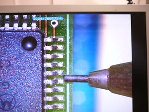
Can I disassemble my source code file?
Yes you can disassemble source code files. To create a disassemble file follow steps given below:

Right-click the source file
A context menu appears.
Select Disassemble from the context menu.
The Disassemble Job window appears.
The disassembling file provides a way to show the results of object code produced from a C/C++ source file in the Editor. Once the Disassemble command is executed,
it will proceed to compile, disassemble the file and show the resulting disassembled file in a new editor window, titled sourcefilenameXXXXX.lst,
where XXXXX represent random numbers.
Decoder V-5.0.20 Build 11006, Jan  7 2011
Options: -A -ArgFilemain.args -C -Env"GENPATH=F:/opt/WORKSPACES/codewarrior/example11_3/Project_Headers;C:\Program Files\Freescale\CW MCU v10.1\eclipse\../MCU/lib/hc08c/device/src;C:\Program Files\Freescale\CW MCU v10.1\eclipse\../MCU/lib/hc08c/lib;C:\Program Files\Freescale\CW MCU v10.1\eclipse\../MCU/lib/hc08c/src;C:\Program Files\Freescale\CW MCU v10.1\eclipse\../MCU/lib/hc08c/device/include;C:\Program Files\Freescale\CW MCU v10.1\eclipse\../MCU/lib/hc08c/include;C:\Program Files\Freescale\CW MCU v10.1\eclipse\../MCU/lib/hc08c/device/asm_include" -EnvOBJPATH=. -EnvTEXTPATH=. -L -Omain.lst -T -ViewHidden -Y
Decoding File: 'F:\opt\WORKSPACES\codewarrior\example11_3\Sources\main.obj'
File format: ELF/DWARF

DISASSEMBLY OF: '.text' FROM 796 TO 929 SIZE 133 (0X85)
Opening source file 'F:\opt\WORKSPACES\codewarrior\example11_3\Sources\main.c'
   26: void mcu_init(void)			// NX  initialize Ports, Clock, Timers, ATD (~ADC), ...Interrupts
mcu_init:
00000000 A602     [2]    LDA    #0x02
00000002 C70000   [4]    STA    SOPT
   34:   ICGC2 = MFDx18;		  //NX bMFD2 | bMFD1 | bMFD0 ==> Multiplication factor 18
00000005 6E7000   [4]    MOV    #0x70,ICGC2
   35:   ICGC1 = ICG_FEI;        //NX FLL Engaged, Internal reference
00000008 6E0800   [4]    MOV    #0x08,ICGC1
   41:   PTDDD = BIT_0 | BIT_1 | BIT_3;  	// PTD0, PTD1 and PTD3 as outputs
0000000B 6E0B00   [4]    MOV    #0x0B,PTDDD
   43:   ATDPE = ANALOG_CH+0x01; // NX PortB.ANALOG_CH pin(s) --> analog input(s)
0000000E B700     [3]    STA    ATDPE
   44:   ATDC  = 0xE0;		      // NX enable, justification-right, 8bit-resolution, left-is-unsigned, 0000-divide-2
00000010 6EE000   [4]    MOV    #0xE0,ATDC
   46:   ATDSC = ANALOG_CH;	  // NX This write starts an new conversion, Using channel ANALOG_CH
00000013 6E0100   [4]    MOV    #0x01,ATDSC
   50:   TPM2SC = 0X08;		  // NX TPM Clock Source to Prescaler Input IS Bus rate clock (BUSCLK) [page 158]
00000016 6E0800   [4]    MOV    #0x08,TPM2SC
   51:   TPM2MOD = 0xFF;		  // NX TPM2 counter maximum value
00000019 AEFF     [2]    LDX    #0xFF
0000001B 8C       [1]    CLRH
0000001C 3500     [5]    STHX   TPM2MOD
   52:   TPM2C1SC = TPM_PWM_HIGH;// NX Input Capture Output Compare
0000001E 6E2800   [4]    MOV    #0x28,TPM2C1SC
   53:   TPM2C1V = 0x00;		  // NX Unlatch the Value register
00000021 5F       [1]    CLRX
00000022 3500     [5]    STHX   TPM2C1V
   56:   TPM1SC = 0X08;		  // NX TPM Clock Source to Prescaler Input IS Bus rate clock (BUSCLK) [page 158]
00000024 6E0800   [4]    MOV    #0x08,TPM1SC
   57:   TPM1MOD = 0xFF;         // NX TPM1 counter maximum value
00000027 5A       [1]    DECX
00000028 3500     [5]    STHX   TPM1MOD
   58:   TPM1C1SC = 0x00;
0000002A 3F00     [5]    CLR    TPM1C1SC
   59:   TPM1C1V = 0x00;		  // NX Unlatch the Value register
0000002C 5F       [1]    CLRX
0000002D 3500     [5]    STHX   TPM1C1V
   61:   TPM1MODH = KHZ_7;		 // NX This 16 bit register is the value that when reached, timer is reset
0000002F 6E0B00   [4]    MOV    #0x0B,TPM1MOD
   62:   TPM1MODL = 0x00;		 // NX 7KHz with 0x0B00, 7.8KHz with 0x0A00
00000032 3F01     [5]    CLR    TPM1MOD
   64:   EnableInterrupts;		 // NX Interrupts enabled but no interrupt used
00000034 9A       [1]    CLI
   65: }//NX mcu_init() ends here
00000035 81       [6]    RTS
   73: void spi_write(char data)
spi_write:
00000036 87       [2]    PSHA
00000037 A7FE     [2]    AIS    #-2
   76:   STROBE = 0;             	    // enable the SPI peripheral
00000039 1700     [5]    BCLR   3,PTDD
   77:   for (temp=8; temp; temp--)  	// repeat eight times
0000003B AE08     [2]    LDX    #0x08
0000003D 8C       [1]    CLRH
0000003E 9EFF01   [5]    STHX   1,SP
   79:     if (data & BIT_7) DATA = 1; else DATA = 0;
00000041 95       [2]    TSX
00000042 E602     [3]    LDA    2,X
00000044 2A03     [3]    BPL    *+5       ;abs = 0x0049
00000046 1000     [5]    BSET   0,PTDD
00000048 651100   [3]    CPHX   #0x1100
   80:     CLOCK = 1;            	    // set the CLOCK pin
0000004B 1200     [5]    BSET   1,PTDD
   81:     data = data << 1;     	    // shift data one bit to the left
0000004D 6802     [5]    LSL    2,X
   82:     CLOCK = 0;            	    // clear the CLOCK pin
0000004F 1300     [5]    BCLR   1,PTDD
   77:   for (temp=8; temp; temp--)  	// repeat eight times
00000051 6D01     [4]    TST    1,X
00000053 2601     [3]    BNE    *+3       ;abs = 0x0056
00000055 7A       [4]    DEC    ,X
00000056 6A01     [5]    DEC    1,X
00000058 9EFE01   [5]    LDHX   1,SP
0000005B 26E4     [3]    BNE    *-26       ;abs = 0x0041
   84:   STROBE = 1;             	    // disable the SPI peripheral,
0000005D 1600     [5]    BSET   3,PTDD
   85: }//NX spi_write() ends here
0000005F A703     [2]    AIS    #3
00000061 81       [6]    RTS
   89: void main(void)
main:
00000062 ADFF     [5]    BSR    mcu_init
   93:   counter = 0;
00000064 4F       [1]    CLRA
00000065 C70000   [4]    STA    counter
   96: 	  if (TPM1SC > 0x7F)		//NX We have timer overflow
00000068 B600     [3]    LDA    TPM1SC
0000006A A17F     [2]    CMP    #0x7F
0000006C 2315     [3]    BLS    *+23       ;abs = 0x0083
   98: 		  TPM1SC = 0X08;        //NX
0000006E 6E0800   [4]    MOV    #0x08,TPM1SC
  100: 	      if(ATDSC > 0x7F)		//NX We have available data from ATD
00000071 B600     [3]    LDA    ATDSC
00000073 A17F     [2]    CMP    #0x7F
00000075 23F1     [3]    BLS    *-13       ;abs = 0x0068
  102: 			  TPM2C1V = ATDRH ;	//NX PWM = ADC
00000077 BE00     [3]    LDX    ATDR
00000079 8C       [1]    CLRH
0000007A 3500     [5]    STHX   TPM2C1V
  103: 			  spi_write(ATDRH); //NX SPI = ADC
0000007C B600     [3]    LDA    ATDR
0000007E ADFF     [5]    BSR    spi_write
  104: 			  ATDSC = ANALOG_CH;//NX Start ADC
00000080 6E0100   [4]    MOV    #0x01,ATDSC
   94:   while(1)						//NX main loop starts here
00000083 20E3     [3]    BRA    *-27       ;abs = 0x0068
MC68HC908JL16
HC08JK-JL: Family [1]
MC68HC908JL16 [2]
In-Circuit Programming of FLASH Memory Using the Monitor Mode for the MC68HC908JL/JK
MC9S08GT16
- 300-page MC9S08GT16A datasheet at Freescale Product page


CodeWarrior
CodeWarrior is the Freescale Software development environment. There is a CodeWarrior suite for every Freescale microprocessor family.
CodeWarrior Product Summary Page
CodeWarrior-Special edition for 08 series has code limit for C programs at 32KB. There are 2 versions.
- The Eclipse-Hosted support only 9S08
- The traditional IDE. support only HC908
- It is very easy to download and install both.
CodeWarrior Download special editions
Serial Memory
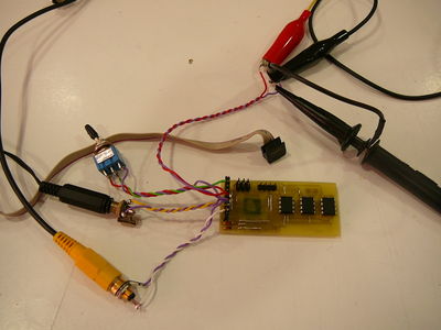
To use as low CPU pins as possible, only serial memory can be used.
For 8KHz sampling rate,
DataFlash with internal SRAM buffers are the only fast-enough Flash devices that can be used. Sizes>4MBit. Erase, Write current consumption is at 30mA levels.
For Lower consumption, FRAM is the smartest solution. But it is single source.
For best availability and cost, a combination of SPI-EEPROM and SPI-SRAM is the best compromise.
FRAM
- FRAM 32K x 8 without write delay and random access Everspin MR25H256 SPI, EEPROM & SerialFlash compatible, very-nice current consumption $4.14@100pcs, $5.66@1pc Digikey, also Arrow, Future, Verical,??EBV??
- Also 1Mbit (128K x 8) version MR25H10
- Good price of 1Mbit MR25H10 at Future Electronics $5.57 / @1pc
- 128KB / sampling-rate =
- 26 sec at sampling rate 4.9 KHz
- 16 sec at sampling rate 8 KHz
- Only one chip, no chip-select glue logic
- No need for CPU RAM buffer in the size of EEPROM page (...128 Bytes)
- No wait time for transferring the recording from SRAM to EEPROM
SRAM
- SPI SRAM 32K x 8 Microchip 23K256 3mA@1MHz
- Digikey [8-DIP] part number: 23K256-I/P-ND $1.66@1pc


STATUS REGISTER
The mode bits indicate the operating mode of the
SRAM. The possible modes of operation are:
0 0 = Byte mode (default operation)
1 0 = Page mode
0 1 = Sequential


INSTRUCTION REGISTER
The 23X256 contains an 8-bit instruction register.
The device is accessed via the SI pin, with data being
clocked in on the rising edge of SCK. The CS pin must
be low and the HOLD pin must be high for the entire
operation.


WRITE
Once the device is selected, the Write command can
be started by issuing a WRITE instruction, followed by
the 16-bit address, with the first MSB of the address
being a “don’t care” bit, and then the data to be written.
A write is terminated by the CS being brought high.

SEQUENTIAL MODE
If operating in Sequential mode, after the initial data
byte is shifted in, additional bytes can be clocked into
the device. The internal Address Pointer is automatically
incremented. When the Address Pointer reaches
the highest address (7FFFh), the address counter rolls
over to (0000h). This allows the operation to continue
indefinitely, however, previous data will be overwritten.
RECORDING SEQUENCE PSEUDOCODE:
- 1 byte to MOSI, INSTRUCTION 'WRITE TO STATUS REGISTER' -->0000 0001 (WRSR)
- 1 byte to MOSI, STATUS REGISTER CONTENT--> 0100 0001 (Sequential mode)
- 1-Byte to MOSI, INSTRUCTION 'WRITE'---> 0000 0010 (WRITE)
- 2-Bytes to MOSI, ADDRESS ---> 0x00
- 1-Byte to MOSI, DATA ---> Data from ADC
- Repeat previous step 8000 times
EEPROM
MICROCHIP
- SPI EEPROM 64K x 8 Microchip 25LC512-I/P : 512 Kbit SPI Bus Serial EEPROM 5mA@10MHz
- Digikey [8-DIP] part number 25LC512-I/P-ND $2.64@1pc
STM
- SPI EEPROM 32K x 8 STM M95256 3mA@1MHz
- No [8-DIP] available
Links
- Telephone Line Interface and Speaker Phone Circuit Austriamicrosystems AS2522b

- 2K Microwire-Compatible Serial EEPROM Microchip 93LC56B
Text to speech
Text to speech here
- Includes Greek Language
2011.07.27 TODO DONE
- ADC--->PWM directly,
- No need to wait the memories to be delivered
- Easy to test different sampling rates and check the quality
- Easy to test in both C and Assembly
2011.07.28
- 9S08GT16A Main Loop: Reads ADC, sends the value to PWM channel, and to bit-banging-SPI
- Not used any interrupt or delay
- Loop frequency is
38.76 KHz7 or 7.8KHz with used timer (TPM1MOD 0x0B00 or 0x0A00) - It is a test without any SPI memories connected (waiting to be delivered)
TODO:Use timer to control the loop-frequency to wanted sampling rate. DONE: With TPM1, not used any interrupt
TODO: Put audio to ADC input and Loudspeaker to PWM DONE
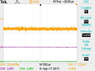
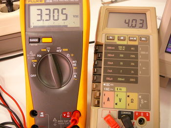
YEL= SPI_MISO, CYAN=SPI_SCK, MAG=SPI_ENABLE, GREEN=PWM ENABLE frequency is38.76KHz7.8KHz and equals to sampling rate. SPI BIT period is 2.6us, PWM frequency is 78KHz The first with low Duty-Cycle PWM and the other 3 with high duty-cycle (low and high ADC input) Below oscillograms for loop-frequency 38.76 KHz.


2011.08.23
- Τested with music, no SPI memories yet.ADC input---PWM output
- Recording SPI is active
- Output filter 1K-100nF
- Sampling rates tested:
- 7 KHz sounds OK
- 6 KHz sounds metallic
- 5 KHz sounds more metallic
- 3.5 KHz sound very metallic
- DC offset needed in input to avoid negative side of sound signal
2011.08.29
- Recording with 4.9 KHz sampling rate video
- first time input ->ADC ->PWM so we can hear what is recorded
- second time SRAM to audio, for debugging
- third time EEPROM to audio. It is the stored recording
- next times are repeats of EEPROM recording (debugging)
- Codewarrior video
- open codewarrior
- edit source
- build project
- start debugging session
- reset target
- run the firmware on target
- record voice message to EEPROM using avatar from internet
- message is played:
- once as inputs to SRAM,
- once more as read from SRAM
- Re-played continuously from EEPROM
- Target board is reset from debugger
- Stops running
- Ready to Run from main
- end of video
2011.08.30
- Second SRAM 32KBytes (EEPROM is 64KBytes)
- Doubles the message duration
- Added to breadboard
- Firmware updated
- MODE switch added
- Mode0 = Playback the EEPOM content
- Mode1 = Record and Playback
- STILL TODO:
- ADD CD4094 functionality
- Now using I/O lines for
- CHIP SELECT of first SRAM
- CHIP SELECT of second SRAM
- CHIP SELECT of EEPROM
- Now using I/O lines for
- Create PCB
- Schematic,PCB, Gerber,
- CNC prototype
- Solder and test
2011.08.31
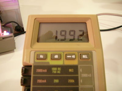
- Run current is in the order of 1mA at BUSCLK 1-2 MHz
- Page 266, A.7 Supply Current Characteristics of 300pages MC9S08GT16A.pdf datasheet
- PWM frequency from 78 KHz reduced to 20 KHz. consumption reduced 0.5mA
- ATD (ADC) is turned of in Playback mode. Consumption reduced 1mA
- With BUSCLK 20 MHz consumption = 16mA
- BUSCLK reduced to 11.111 MHz---> consumption < 11 mA
- Can not reduce more the BUSCLK due to bit-banging SPI speed
- 32 bit SPI transaction takes more time than the 4.9 KHz sampling period if BUSCLK < ~10 MHz
- Using SPI peripheral could solve this
- Fast SPI transaction will reduce the active time --->
- Sleep mode could reduce drastically the total consumption
- Timer Interrupt must be used instead Timer Flag polling from main-loop
| VDD Volt |
Consumtion mA |
Conditions |
| 3.6 |
12 |
|
| 2.9 |
9 |
1 x 1N4148 IN SERIES 3.6V TO VDD |
| 2.2 |
7.5 |
2 X 1N4148 IN SERIES 3.6V TO VDD |
| VDD Volt |
Consumtion mA |
Conditions |
| 3.3 |
10 |
|
| 2.6 |
8.7 |
1 x 1N4148 IN SERIES 3.3V TO VDD |
| 1.93 | 6.26 | 2 X 1N4148 IN SERIES 3.3V TO VDD |
- Include two 1N4148 in series with supply to control the supply-voltage
- Can bridge one or both
- So by applying to board 3.3V, VDD can be:
- 3.3V or
- 2.6V or
- 1.93V
Only 5 mA
- -------------------------- !!! AVAILABLE CURRENT IS 5mA !!!! -----------------------------------
- Change Software to use
- tick-interrupt DONE/TESTED
- SPI peripheral initialize DONE/TESTED
- Do not use GPIO SPI lines DONE/TESTED
- Modify low level SPI drivers DONE/TESTED
- Reduce BUSCLK to 4 MHz then 2 MHz and since they are now changed:
- Change tick timer value --------------> 4.9 KHz DONE/TESTED
- Change PWM to ------------------------> 20KHz DONE/TESTED
- Change SPI timing so 4 x 8 bit -------> 32us DONE/TESTED
- low-power mode
- Change Hardware
- SRAM2 line CS1 move from PTE3 to PTA7 DONE/TESTED
- MODE line move from PTE2 to PTA4 DONE/TESTED
- MOSI line move from PTD0 to PTE4/MOSI1 DONE/TESTED
- MISO line move from PTC5 to PTE3/MISO1 DONE/TESTED
- SCK line move from PTD1 to PTE5/SPSCK1 DONE/TESTED
| VDD Volt |
Consumtion mA |
Conditions |
| 3.3 |
5.7 |
|
| 2.6 |
4.3 |
1 x 1N4148 IN SERIES 3.3V TO VDD |
| 1.93 | 3.3 | 2 X 1N4148 IN SERIES 3.3V TO VDD |
| VDD Volt |
Consumtion mA |
Conditions |
| 3.3 |
4.3 |
|
| 2.6 |
3.3 |
1 x 1N4148 IN SERIES 3.3V TO VDD |
| 1.93 | 2.5 | 2 X 1N4148 IN SERIES 3.3V TO VDD |
------------------ Below test results are GOOD ----------------------
| VDD Volt |
Consumtion mA |
Conditions |
| 3.3 |
3.8 |
|
| 2.6 |
2.8 |
1 x 1N4148 IN SERIES 3.3V TO VDD |
| 1.93 | 2.15 | 2 X 1N4148 IN SERIES 3.3V TO VDD |
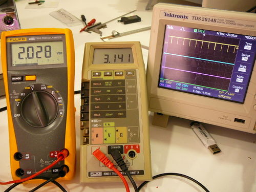
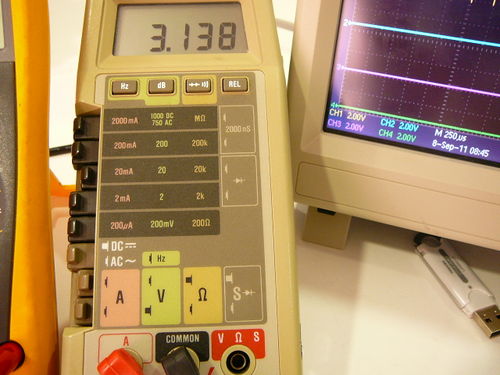
2011.09.01
- PLAY MODE is OK but RECORD-MODE is not working
- Reduced BUSCLK and SPI peripheral combination creates problem!!!!
TODO: *********FIND WHY***********DONE (after 12 hours of debugging)- ....SPI is still transmitting after the software is gone...
- Transmit Empty Flag means that register is empty. Transmission is still active
- Receiver Empty Flag seems to be the solution, but both polling and interrupt attempts did not work (??yet??)
- Now that the problem can be checked with oscilloscope, can proceed with a WORKAROUND.
- ....SPI is still transmitting after the software is gone...
*WORKAROUND
void spi_wr(unsigned char data){	//
	  volatile  unsigned temp; 					//
	  temp = SPIS;
	  SPID = data;

	  temp = SPIS;
	  while ( (temp & bSPRF) == 0 ){temp = SPIS;}	// Can not read the bit, only works as delay *******WORKAROUND
	  temp = 0; // some more delay (~2us) needed for the page write of eeprom **************************WORKAROUND
}
- SPI know-how, tests on
- How to tune tick period, SPI timing, Delays for different BUSCLK
- SPTEF, SPRF Flags
- SPI interrupt
- SPI EEPROM
- How to handle EEPROM-BUSY during page-write
- Reading status register
- With delay
- So many tests created a confusion with working, not working versions and which version doing-what. As a solution tested:
- Use a version control system inside eclipse-codewarrior


- Have a different project for every version of firmware
- Can easily test all versions and compare results
- TODO:
- As STOP3 mode is not working (yet) and WAIT mode (tested) offers not-so-big consumption improvement:
- Try to reduce BUSCLK just after every SPI transaction
- The active time is 32us and the total period of main loop is 200us (the sampling rate)
- Running with reduced BUSCLK after the first 32us might reduce consumtion
- Try to reduce BUSCLK just after every SPI transaction
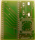
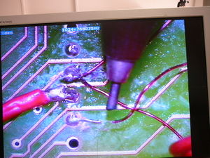
- PCB:
Place a picture of PCB in WIKI- Finalize the PCB
2011.09.02
- PCB DIMENSIONS 65 X 28.5mm
- PCB 3D VIEWS


- PCB SCHEMATIC
- To be updated.
- Now SPI peripheral is used
- Different pins used for SPI
- How to communicate with HOST HC908JL16???????
- Now SPI peripheral is used

*Firmware versions history
//V007
//stop tick during EEPROM write
//Rename BUSY_LED to TP1, Do not use anywhere except...
//Use TP1 only in TICK interrupt
//increase TICK to 4.4KHz, WE can stay with this.
//SAMPLING_RATE 0x01 0xB8
//4.9 KHz Fails to write in SRAM  ??? WHY ???
//CONSUMPTION IS 3.5 mA(EEPROM WRITE AND READ) AND 4 mA (SRAM WRITE AND READ) *** AT 2 V ***
//We have to go with 2V VDD. It is inside the low VDD limits of all ICs
//Still with zero input recording is very quiet :)
//With audio connection to PC audio output and no sound we have "background" noise ?????? WHY ???????
//The used sound from PC has too many high frequency components to 's'. It is digitally synthesized.
//In PCB To use 2 stages better passive filter in output (now single stage) and to input (now without filter)
//Tested input single stage low-pass filter (Anti-aliasing) 200nF+3.9K, Output filter (single stage low-pass for PWM) 200nF+1K  <<<<Quality is improved, no 'background' noise, 's' sounds better
//Some metallic tone in voice still exists
//Input DC bias voltage set to 500 mV
//

//V006
//ICGC2 = MFDx4 | RFD_DIV2;          instead ICGC2 = MFDx10;   in V005
//spi_wr(), spi_read() all delays removed
//SPIBR = SPI_PRE1 | SPI_DIV2;
//SAMPLING_RATE 0X02 0X00 **3.9 KHz**, difficult to increase
//Test RECORDING with no input signal is very silent :)

//V005 ONLY MINOR CHANGES (REMOVE UNUSED VARIABLES)

//V004 FROM V002B
//SPI working SPTEF can not be read. for read it does not matter,  --->Is transmit register empty, means register can accept data BUT TRANSMITION still ACTIVE!
//so no use as end of transmission
//affects only the last byte of every sector???
//For write matters when EEPROM sector is massively written. In this case the bytes go one after the other and not in the sampling-rate frequency
//*** During EEPROM writing, Can seen in oscilloscope that SPI clock still plays after EEPROM CS is de-activated (=high)***
//Some delay (~2us) needed then
//Can not use the tick as it is in the 200us period
//SPRF tested and did not work
//SPRF interrupt tested, did not work
//Remain with the delay <<< does not matter, with lower BUSCLK have to remove the delays....check higher versions


//V002 GPIO PORTS INITIALISATION NOW CORRECT
Characteristics, Performance
- Firmware is mostly done
- Sampling rate 4.4 KHz
- VDD = 2V, Created with voltage-drop diodes 1n4148 from Supply Voltage 3.3V
- Consumption
- Playback 3.5mA
- Recording
- During SRAM access 4 mA
- During EEPROM access 3.5 mA
- PCB dimensions 65 x 28.5 mm
- CPU MC9SGT16A QFP44 (e=0.8mm)
- SRAM 2 x Microchip 23K256-I/P DIP-8
- EEPROM 1 x Microchip 25LC512-I/P DIP-8
- Message Duration: 14.7 sec (65 535 bytes / 4400 samples/sec =14.77 sec)
- ACTIVATION<<<<<<<<TO BE RE-DEFINED
- Power-ON
- If MODE Input is high
- Record,
- Play During recording, this will create audio-feedback if used with microphone. Will change
- Play from RAM
- Store to EEPROM
- Play from EEPROM again and again
- If MODE Input is LOW
- Play from EEPROM again and again
- Record,
- If MODE Input is high
- Sound quality, Supply Voltage and Current consumption ***** VIDEO *****
2011.09.03
- Schematic updated
- CS0, CS1, CS2 to different CPU pins due to pcb-layout
- RESET and MODE lines for activation of RECORDING or PLAYBACK
- TP1, TP2, and MODE lines can all be used as INTERRUPT source for the CPU
- So an interrupt driven SPI slave can be easily implemented in Firmware
- ...If this is convenient for HOST
- So an interrupt driven SPI slave can be easily implemented in Firmware
- PCB design is finished
- Final dimensions slightly enlarged: 67.5mm X 30mm
- Single layer with Jumpers
- ALL PADS are enlarged as possible, to use
- CNC copper removal
- Or DIY etching


2011.09.04
- PCB engraving
- FAILED, TOO DENSE PCB ... :(


2011.09.05
- ALL FILES TO REPRODUCE THE PROJECT ARE NOW DOWNLOADABLE
- PCB
- Schematic and PCB CAD files
- Gerber
- GCODE for engraving
- FIRMWARE
- S19 to program CPU
- Complete CODEWARRIOR project
DOWNLOAD
2 OR 3 LEVELS OF COMPRESSION USED TO AVOID SERVER FILE-BLOCKING
- DOWNLOAD GERBER/DRILL FILE-SET: File:Voice08.tar
- DOWNLOAD S19 FILE File:Voice08 s19.tar
- DOWNLOAD CODEWARRIOR_10.1 PROJECT File:Voice08 V008.tar.gz
- DOWNLOAD SCHEMATIC AND PCB FILES File:V08A.tar.gz
- DOWNLOAD GCODE FOR CNC PCB ENGRAVING File:Engrave.tar.gz. For 30'(degrees) tool
- DOWNLOAD THIS WIKI IN PDF File:Wiki.gz
Printable version of WIKI
- Click 'Printable version' at the left side of WIKI, then print to printer (or to PDF if available in your PC)
TODO
- Purchase new chemicals for PCB to try the 'standard' method
PCB
- After 8 hours yesterday and 6 hours today, still can not have a prototype pcb using CNC or Chemicals!
- What to do next:
- Use an already existing QFP44 Adapter-PCB from other project
- Place the 3 memory chips on a drilled-board and have a second prototype for testing
- Order processional PCB (2pcs, total cost:74 EU +VAT) with green masks and silkscreen
- Ordering today, to be delivered 2011.09.12

2011.09.06
- Second Prototype worked after 8 hours of soldering and testing:
- R E A D Y - T O - D E M O

- Check movie
- New PCB design is ready
- Small dimensions 32.5mm X 28.7mm
- All SMD


- Updated Schematic

2011.09.07
intelco tests
- intelphone current consumption from telephone line at level 25mA
- This is more than expected!!
- current can be reduced by increasing AMSxxxx 30Ω loop-sense-resistor.
- This resistor controls the loop-current
- Increase from 30 to 330 ohm gave a current reduction about 4-5 mA
- These 5 mA are OK to power voice08 board
- Tested value 600 Ohm: intelphone does not start
- Voice08 board (2nd prototype) appears to consume ~17 mA at 2 V supply
- This high consumption is malfunction
- Normal consumption is 4 mA MAX at 2 V
- CPU gets warm
- This high consumption is malfunction
- Voice08 tested successfully at PLAY mode (standalone)
How to proceed
In one week timescale:
- Repair 2nd prototype
- Test 2nd prototype with intelphone
- Design pcb and build new version3 prototypes
For Today
- Test Loop-sense-resistor values between 330 and 600 Ω
- Try to add a 5 mA resistive load to intelphone to test how much current can supply for voice08 board (400Ω at 2V)
- Measure voice08 board current with oscilloscope and 1Ω shunt-resistor
- Repair voice08 board
- Redesign voice08 board in dimensions that feat inside intelphone box
- Order (bakis) from Digikey all needed parts for new prototypes
- To be delivered in one week
Up to next Wednesday
- Make the board at intelco lab
- Postscript format if possible from Altium
- PDF if can be printed in the right dimensions
- Get the ordered parts from Bakis
- Assembly and test version 3 board(s)
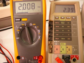
Tests on 1st prototype
- Current consumption on first prototype measured again for confirmation
- .
- .
- It is as expected


Tests on 2nd prototype
- ------------- Current consumption on 2nd prototype is higher than normal -------------
- .
- Supply current measured on 1Ω shunt-resistor to supply-line
- .
- .
- Suspected a GPIO bit shorted to VDD
- Found to be the PTA7

- .
- By removing initialization of BIT_7, the consumption is restored to normal value
- .
- Pins 40,39 (VDD,PTA7) were short-circuit
- ...By mistake. Here repaired:
- .


- The Reason of the problem:
- At last moment Port A was all initialized as outputs (except MODE input PT4) to avoid having floating unused inputs
- Having short-circuit VDD-PTA7
- PTA7 initialized as OUTPUT with value ZERO
- ...Current was not measured
- 2nd Prototype is repaired.
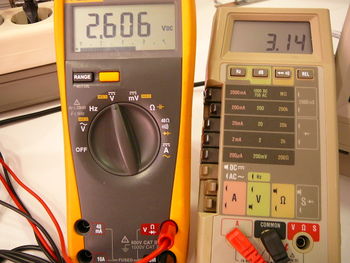
- .
- Current consumption is now even better than the 1st prototype!!!
- At 2 V, it is almost 1 mA less (2.4 mA instead 3.5 mA)


PCB


- Redesigned PCB with DIP memories to feat inside the intelphone box
- MAKE PCB
- Download PDF for film-print File:V08A PCB.pdf
- Just print pdf with Page scaling: None
- Exact dimensions are: 63.04mm x 30.1mm
2011.09.20
- 2 Boards received
- Parts received
- One pcb assembled , to be tested today


2011.09.21
- One board tested
- Everything OK


- If Amplifier will needed:
TSV612
- 10 μA
- Dual, 8 pin, SO8
- Supply 1.5-5.5 V, Current 12μA/channel
- TSV612 digikey price $1.3
TL062
- 200 μA
- TL062 Low-power JFET dual operational amplifiers ST datasheet
- At digikey price $0.67
2011.10.05 Intelco meeting
- Define serial protocol
- Communication between boards intelphone and voice08
- 3 commands from intelphone to voice08
- PLAY
[02]01
- REC
[03]02
- STOP
[04]03
- PLAY
- From voice08 to intelphone:
- ACK [01]
logic
- LOW and HIGH pulse duration 10ms
- IDLE = Logic-HIGH
- ACTIVE = Logic-LOW
- STOP =
90ms100ms extension of last 10ms pulse - HOST:
- If active then wait for 200ms
physical
- SINGLE WIRE
- Bidirectional
- Open collector
doc


2011.10.27
- PC Software:
- Send commands to voice08 board
- Easy for testing
- can be expanded with more commands if needed

- Commands:
- PLAY = 1 pulse + 100ms STOP
- REC = 2 pulses + 100ms STOP
- CUT = 3 pulses + 1000ms STOP
- Acknowledged from board voice08 with:
- ACK = 100ms pulse transmitted from board voice08


- Connection to PC serial port
- Only line DTR is used
- Diode + 3.9K in series, block serial port negative voltage
- Pull-up resistor allows bidirectional operation (22K used here, ...attention with current consumption)


- Functionality
- Recording time:
- Up to 14.4 sec
if STATE is IDLE:
- Command REC -> STATE = RECORDING
- ACK pulse
- Returns to State IDLE
- .
- Command PLAY -> STATE = PLAYING
- ACK pulse
- Returns to State IDLE
- .
if STATE is RECORDING:
- Command CUT
- Mark the Address
- Stop writing to RAM and start copying RAM to EEPROM
- While writing to EEPROM Commands are not accepted
- ACK pulse
- Returns to State IDLE
HCS08 (BDM) Debug and Flash-programming Tools
SPYDER under-test
SOFTEC SPYDER Low Cost BDM tool is EOL (Freescale Status End Of Life completed].

DO NOT USE IT
USBDM
USBDM Is open source, supported by CodeWarrior, Easy to make as many as you like, easy to buy.
It is the physical successor of previous open-source BDM tools: TBDML, OSBDM.
Supports HCS08, HCS12, ColdFire-V1. Does NOT support HC08
Standalone FlashProgrammer Utility
 The minimal version is based on 20SOIC USB device MC9S08JS16CWJ (Mouser $1.92 @ 1pc) + 74LV125AD +12MHZ xtal + PESD5V0S2UA protection + passive. * FREE *

 Buy Commercial-version USBDM in Europe: Flashgenie USBDM JM60 Programmer / Background Debug Module . AT 37EU


USB BDM MULTILINK [TESTED]
Part Number USB-ML-12From PE-micro and Freescale For HCS08,HC12,HCS12,ColdfireV1. Older version blue-colored, current version magenta. At $99.

Nice to work with. [forget mon08 :) ]
CYCLONE-PRO
PE-micro CYCLONE-PRO Standalone toll. At $499.
